General Description
The RT9120S is a high efficiency, I2S-input, stereo channel audio power amplifier delivering maximum 2x30W into 8Ω BTL speaker loads. It can deliver over 94% power efficiency at 2x10W and eliminate the need for heatsink. The built-in anti-pop functions can reduce the speaker’s pop noise under all kind of scenarios. Built-in protection circuits can provide over-temperature, over-current, over-voltage, under-voltage protections and report error status. The RT9120S is a 3-wired device receiving all clocks from external sources with standard I2S, Left-justified, Right-justified or TDM formats. It can support wide input sampling rate from 8kHz to 192kHz. The RT9120S features one band DRC and flexible input mixer, and power clipping.
Performance Specification Summary
Summary of the RT9120S Evaluation Board performance specificiaiton is provided in Table 1. PVDDL = PVDDR = AVCC = 12V, DVDD = 3.3V, RL = 8Ω, TA = 25C, fSW = 384KHz, L = 10µH, C = 0.47µF, unless otherwise specified.
Table 1. RT9120S Evaluation Board Performance Specification Summary
|
Specification
|
Test Conditions
|
Min
|
Typ
|
Max
|
Unit
|
|
Input Voltage Range
|
|
4.5
|
--
|
26.4
|
V
|
|
PVDDL/R+AVCC Quiescent Current
|
PWDNN = 3.3V, switch 50% duty , no load, no LC filter
|
--
|
20
|
25
|
mA
|
|
PVDDL/R+AVCC Shutdown Current
|
PWDNN = 0.8V, no load, no LC filter
|
--
|
--
|
20
|
µA
|
|
Startup Time from Shutdown
|
Excluding volume ramp
|
--
|
80
|
--
|
ms
|
|
Shut Down Time from Enable
|
Excluding volume ramp
|
--
|
60
|
--
|
ms
|
|
PWM Switching Frequency
|
384kHz mode
|
--
|
384
|
--
|
kHz
|
|
RMS Output Power
|
THD+N = 10%, (BTL), PVDD = 12V, RL = 8Ω
|
9
|
10
|
--
|
W
|
|
Total Harmonic Distortion + Noise
|
PO =1W (BTL)
|
--
|
0.03
|
0.1
|
%
|
|
Output Integrated Noise
|
20Hz to 20kHz, A-weighted.
|
--
|
35
|
--
|
µV
|
|
Output Offset Voltage
|
PVDD = 12V, Disable DC Calibration
|
-6.5
|
--
|
6.5
|
mV
|
|
PVDD = 12V, Enable DC Calibration
|
-5
|
--
|
5
|
|
Cross-Talk
|
Output power = 1W, with shielding choke
|
--
|
100
|
--
|
dB
|
|
Signal-to-Noise Ratio
|
THD + N = 1%, PVDD = 24V
|
--
|
113
|
--
|
dB
|
|
Power Supply Rejection Ratio
|
Frequency @1kHz
|
--
|
-75
|
--
|
dB
|
|
Dynamic Range
|
Input level -60dBFS, PVDD = 24V
|
--
|
113
|
--
|
dB
|
|
Efficiency
|
Output power = 10W + 10W
|
--
|
94
|
--
|
%
|
Note: Measurements were made using the RT9120S_EVM board and Audio Precision System 2722 with AUX-0025 low-pass filter.
Operations
1. Connect input power supply (4.5V < PVDD < 26.4V) and ground to PDD and GND pins respectively.
2. Connect input power supply (3.3V) and ground to DVDD and GND pins respectively.
3. The 2X5 Header I2S source input to JP2 (PIN4 = LRCK, PIN6 = SCLK, PIN8 = SDI, PIN10 = SDO).
4. The 2X3 Header I2C source input to J2 (PIN1 = PVSS, PIN3 = SCL, PIN5 = SDA).
5. The 1X3 Header (JP7) is the PWDNB. (JP7, Short PIN1;2 = Disable, Short PIN2;3 = Enable).
6. The 1X3 Header (JP11) is the MUTE_N. (JP11, Short PIN1;2 = Disable, Short PIN2;3 = Enable).
7. The 1X3 Header (JP8) is the FAULTB.
8. The 1X3 Header (JP9, JP25) is the A_SEL. (JP9 is for the 600kΩ use, Short PIN1;2 = 1A, Short PIN2;3 = 1B, JP25 is for the 0Ω use, Short PIN1;2 = 18, Short PIN2;3 = 19 ). See Table 2.
9. The R24/R25 0Ω connect in series is PBTL-mode.
10. Connect speaker to the GP5 (OUT_PL),GP6 (OUT_NL),GP7 (OUT_NR), GP8 (OUT_PR).
Table 2. A_SEL Setting
|
A_SEL
|
Slave Address
|
|
To DVDD
|
0011001
|
|
To GND
|
0011000
|
|
600kΩ to DVDD
|
0011011
|
|
600kΩ to GND
|
0011010
|
Detailed Description of Hardware
Headers Description and Placement
Carefully inspect all the components used in the EVB according to the following Bill of Materials table, and then make sure all the components are undamaged and correctly installed. If there is any missing or damaged component, which may occur during transportation, please contact our distributors or e-mail us at evb_service@richtek.com.
Test Points
The EVB is provided with the test points and pin names listed in the table below.
|
Test Point/
Pin Name
|
Signal
|
Comment (expected waveforms or voltage levels on test points)
|
|
SDA/SCL
|
I2C Signal
|
These two pins are I2C communication between RT9120S and Micron.
|
|
SDI
|
12S Signal
|
12S data input
|
|
LRCK
|
12S Signal
|
12S LRCK input
|
|
SCLK
|
12S Signal
|
12S SCLK input
|
|
DVSS
|
Ground
|
Ground for digital circuits.
|
|
VR_DIG
|
Power
|
1.8V digital supply voltage generated by internal LDO.
|
|
DVDD
|
Power
|
3.3V, 1.8V power supply for I/O.
|
|
AVSS
|
Ground
|
Ground for analog circuits.
|
|
AVCC
|
Power
|
4.5V to 26.4V power supply for analog circuits.
|
|
VR.ANA
|
Power
|
5V analog reference voltage by internal LDO.
|
|
GVDD
|
Power
|
5V power supply generated by internal LDO.
|
|
BSTPR
|
Power
|
Bootstrap supply for VOUTPR.
|
|
VOUTPR
|
Power
|
Positive output of R-Channel.
|
|
PVDDR/PVDDL
|
Power
|
4.5V to 26.4V power supply for R-Channel and L-Channel.
|
|
VOUTNR
|
Power
|
Negative output of R-Channel.
|
|
BSTNR
|
Power
|
Bootstrap supply for VOUTNR.
|
|
BSTNL
|
Power
|
Bootstrap supply for VOUTNL.
|
|
VOUTNL
|
Power
|
Negative output of L-Channel.
|
|
VOUTPL
|
Power
|
Positive output of L-Channel.
|
|
BSTPL
|
Power
|
Bootstrap supply for VOUTPL.
|
|
MUTE_N
|
Setting for mute
|
Mute pin
|
|
FAULTB
|
Informing Event
|
This pin will be low to inform I2C master.
|
|
A_SEL
|
Setting for I2C Address
|
Connect this pin to with the dedicate resisters.
|
|
SDO
|
12S Signal
|
12S data output
|
|
PDWNN
|
Setting for Power Down
|
Power down pin, low active.
|
|
PVSS
|
Ground
|
Ground
|
Bill of Materials
|
Reference
|
Count
|
Part Number
|
Description
|
Package
|
Manufacturer
|
|
AVCC, AVSS, DVSS
|
3
|
WR08X000PTL
|
0/0805
|
0805
|
WALSIN
|
|
C1, C7, C16, C22
|
4
|
0603B474K500CT
|
0.47µF/50V/X7R/0603
|
0805
|
WALSIN
|
|
C3, C11, C13, C21
|
4
|
0603B474K500CT
|
0.47µF/50V/X7R/0603
|
0603
|
WALSIN
|
|
C8, C14, CB3, CB6, CT2, CT9
|
6
|
0603B104K500CT
|
0.1µF/50V/X7R/0603
|
0603
|
WALSIN
|
|
C9, C15, C23
|
3
|
0603X105K250CT
|
1µF/25V/X5R/0603
|
0603
|
WALSIN
|
|
CB1
|
1
|
0805B105K500CT
|
1µF/50V/X7R/0805
|
0805
|
WALSIN
|
|
CB4, CB7, CT1, CT8
|
4
|
0603B102K500CT
|
1nF/50V/X7R/0603
|
0603
|
WALSIN
|
|
CB5, CT3, CT4, CT10, CT11
|
5
|
GRM32ER71H106KA12L
|
10µF/50V/X7R/1210
|
1210
|
MURATA
|
|
CN3, CN4
|
2
|
ED555_2DS
|
ED555_2DS
|
7.0x6.5mm
|
On Shore Technology Inc.
|
|
CT15
|
1
|
GRM32ER71H106KA12L
|
10µF/50V/X7R/1210
|
1210
|
MURATA
|
|
EC2
|
1
|
35ZLH390MEFC8X20
|
390µF/35V
|
Radial
|
RUBYCON
|
|
GP2
|
1
|
GOLD PIN
|
OUT_PL
|
|
BO-JIANG
|
|
GP3
|
1
|
GOLD PIN
|
OUT_NL
|
|
BO-JIANG
|
|
GP4
|
1
|
GOLD PIN
|
OUT_NR
|
|
BO-JIANG
|
|
GP5
|
1
|
GOLD PIN
|
OUT_PR
|
|
BO-JIANG
|
|
GP6
|
1
|
GOLD PIN
|
3.3V/1.8V
|
|
BO-JIANG
|
|
GP7
|
1
|
GOLD PIN
|
PVDD
|
|
BO-JIANG
|
|
GP10, GP11, GP13
|
3
|
GOLD PIN
|
PVSS
|
|
BO-JIANG
|
|
J2
|
1
|
|
HEADER3X2
|
HEADER3X2
|
Cherng Weei
|
|
J9
|
1
|
3111
|
PVDD
|
Binding Post, Medium
|
DA KOANG CO.,LTD.
|
|
J10
|
1
|
3111
|
PVSS
|
Binding Post, Medium
|
DA KOANG CO.,LTD.
|
|
JP1
|
1
|
|
HEADER12X2
|
|
Cherng Weei
|
|
JP2
|
1
|
|
HEADER5X2
|
|
Cherng Weei
|
|
JP3
|
1
|
|
SIP-5P
|
|
Cherng Weei
|
|
JP4, JP5
|
2
|
|
SIP-2P
|
|
Cherng Weei
|
|
JP6
|
1
|
|
GPIO 0
|
|
Cherng Weei
|
|
JP7
|
1
|
|
PWDNB
|
|
Cherng Weei
|
|
JP8
|
1
|
|
FAULTB
|
|
Cherng Weei
|
|
JP9
|
1
|
|
A_SEL
|
|
Cherng Weei
|
|
JP10
|
1
|
|
GPIO 1
|
|
Cherng Weei
|
|
JP11
|
1
|
|
MUTE_N
|
|
Cherng Weei
|
|
L2, L4, L6, L8
|
4
|
7443321000
|
10µH
|
|
Würth Elektronik
|
|
R12, R15, R23
|
3
|
WR06X000 PTL
|
0/0603
|
0603
|
WALSIN
|
|
R13
|
1
|
WR06X1002FTL
|
10k/0603
|
0603
|
WALSIN
|
|
TP9
|
1
|
|
GVDD
|
|
PINGOOD
|
|
TP10
|
1
|
|
FAULTB
|
|
PINGOOD
|
|
TP11
|
1
|
|
VR_DIG
|
|
PINGOOD
|
|
TP12
|
1
|
|
VRANA
|
|
PINGOOD
|
|
U1
|
1
|
RT9120SGQV
|
RT9120SGQV
|
VQFN-32L 5x5
|
RICHTEK
|
|
Z1, Z2, Z3, Z4
|
4
|
|
FK_1
|
|
|
|
Z5, Z6, Z7, Z8
|
4
|
TCK-17
|
SIP-1P-M
|
|
PG
|
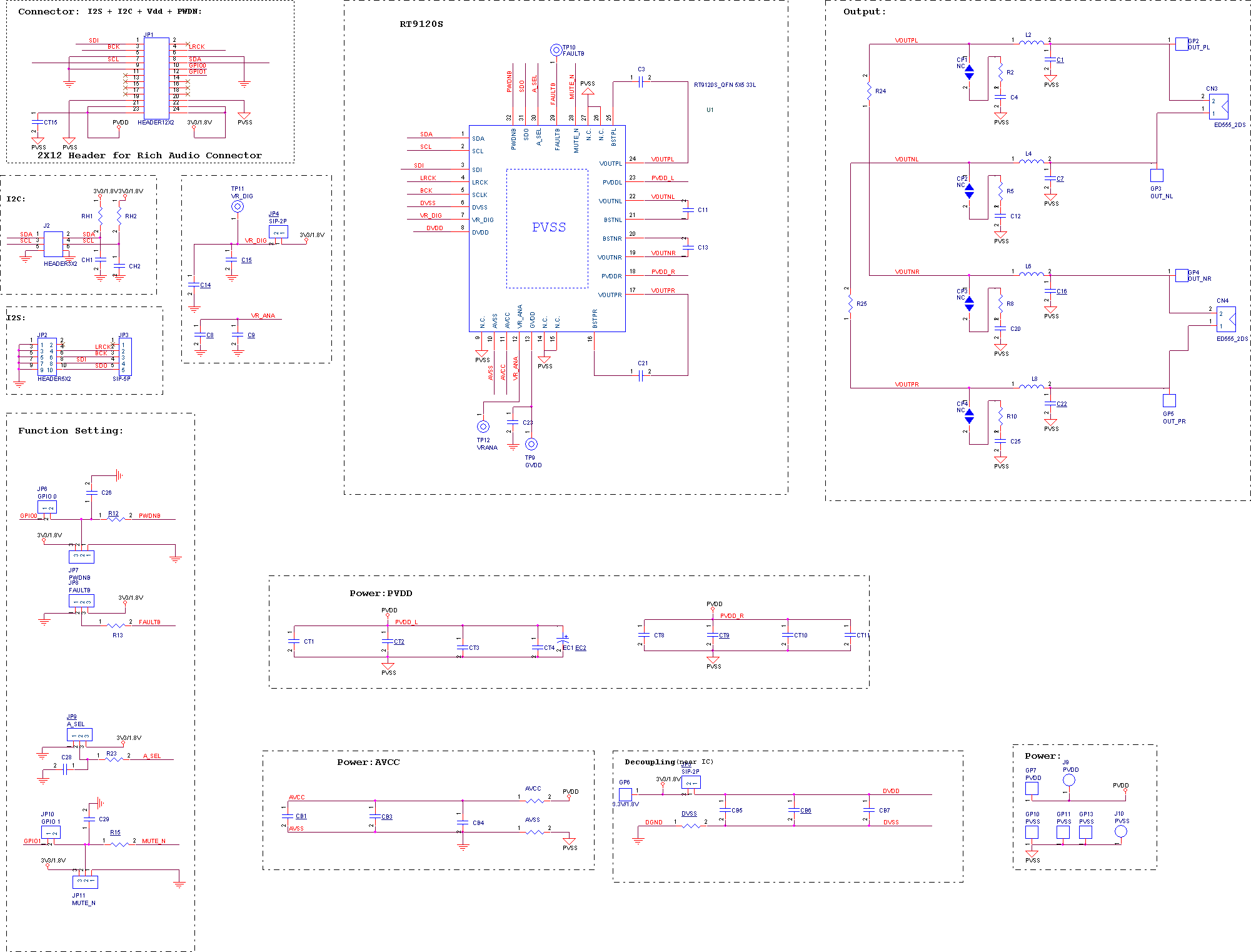
Typical Applications
EVB Schematic Diagram
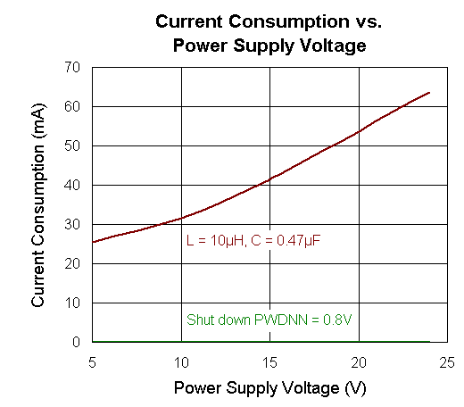
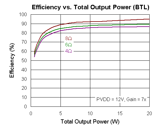
Measure Result
PWM = 384kHz
|
Current Consumption vs. Power Supply Voltage
|
Efficiency vs. Total Output Power (BTL)
|
|
|
|
|
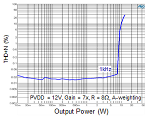
THD + N vs. Output Power (BTL)
|
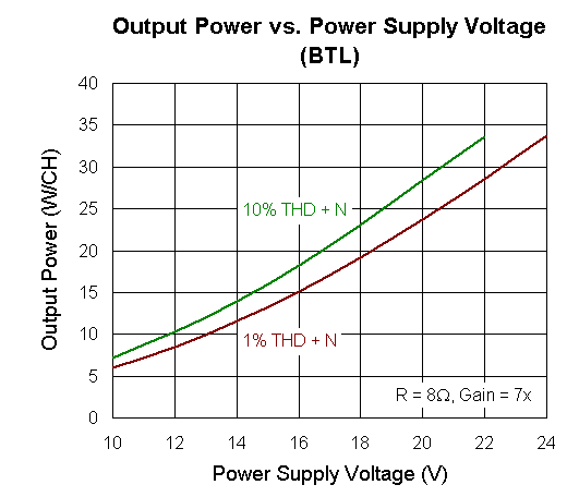
Output Power vs. Power Supply Voltage (BTL)
|
|
|
|
|
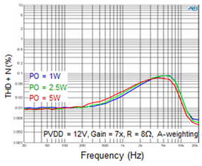
THD + N vs. Frequency (BTL)
|
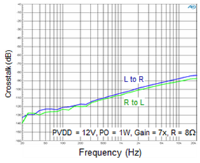
Crosstalk vs. Frequency
|
|
|
|
|
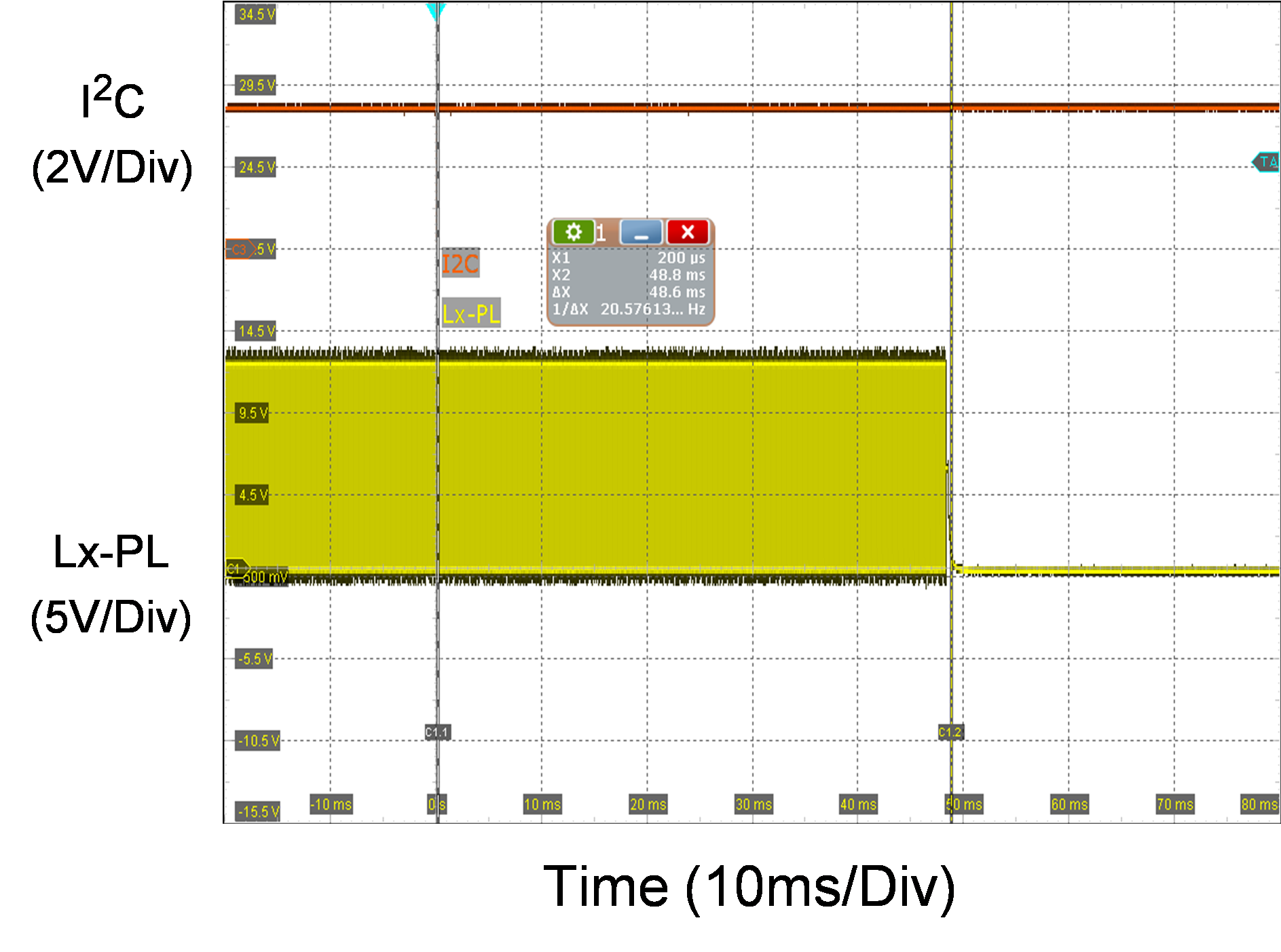
Startup Time from Shutdown
|
Shutdown Time from Enable
|
|

|
|
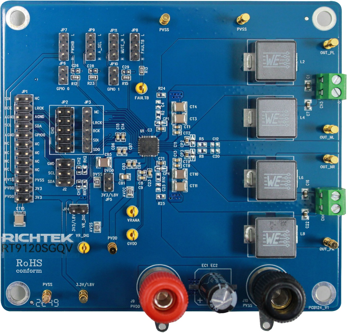
Evaluation Board Layout
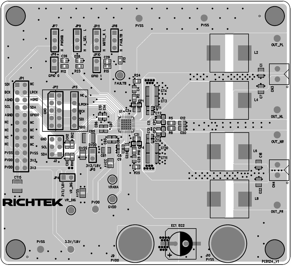
Figure 1. Top View (1st layer)
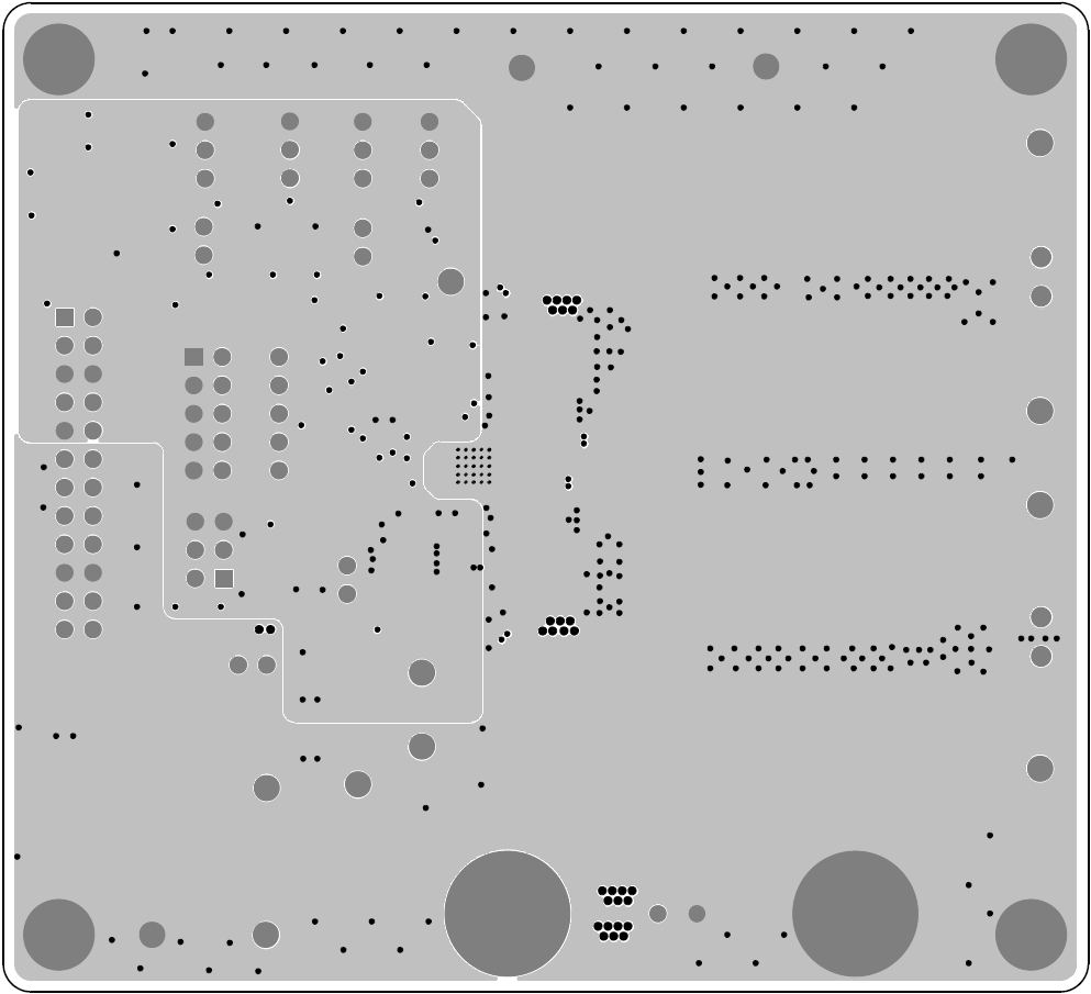
Figure 2. PCB Layout—Inner Side (2nd Layer)
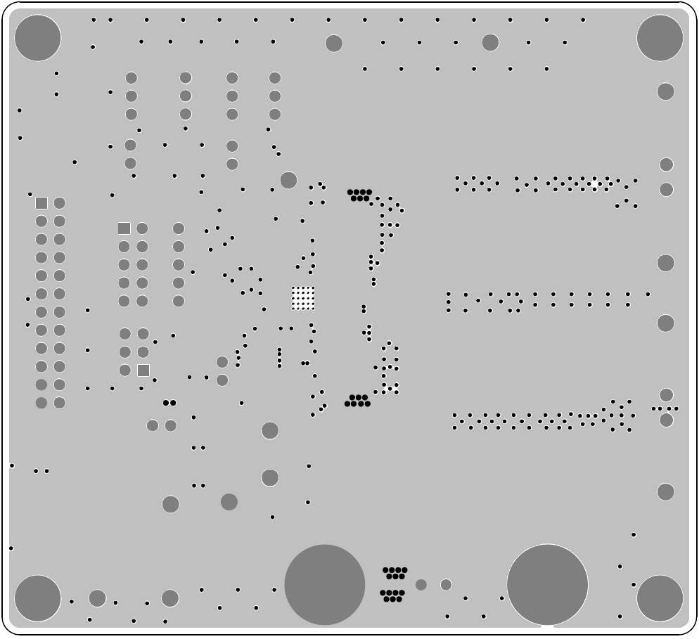
Figure 3. PCB Layout—Inner Side (3rd Layer)
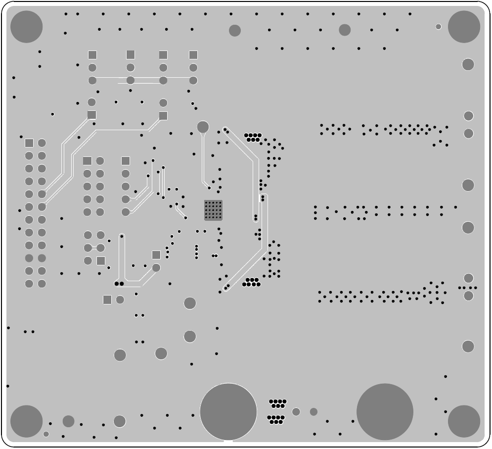
Figure 4. Bottom View (4th Layer)